
Hardware

worlds smallest chip

Worlds Smallest Chip

Worlds Smallest Chip Isn’t the Biggest Breakthrough IBM recently unveiled what it describes as the world’s smallest chip, featuring transistor channels only about 15 silicon atoms wide. At first glance, this achievement appears to be another milestone in the decades-long race to make transistors smaller. Yet the most significant innovation isn’t the transistor’s tiny dimensions. […]

Worlds Smallest Chip Read More »
Chinas-EUV-Breakthrough

China’s EUV Breakthrough

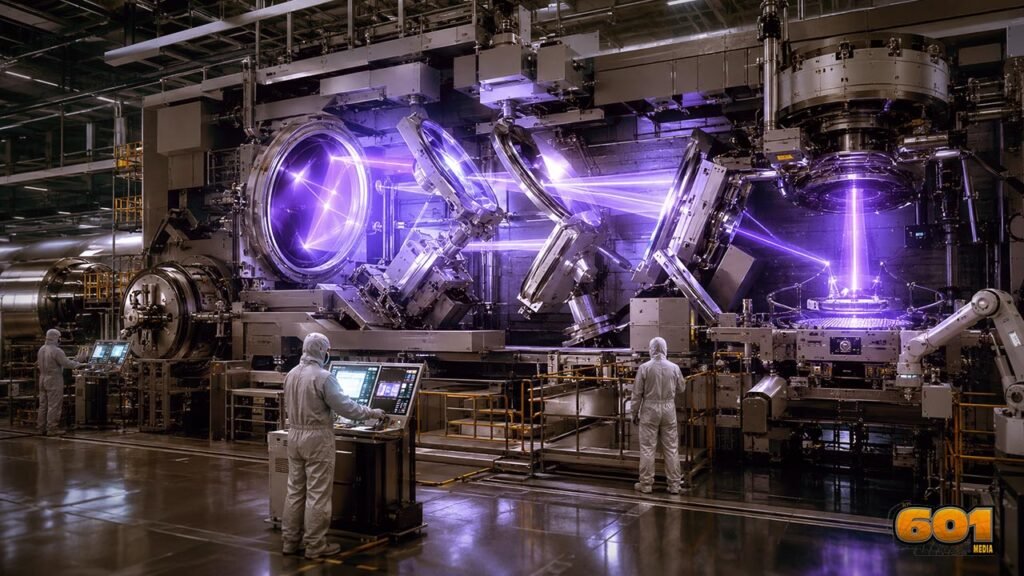
China’s EUV Breakthrough: The Long Road to Semiconductor Independence China’s effort to develop its first domestically built Extreme Ultraviolet (EUV) lithography machine represents one of the most ambitious engineering projects in modern semiconductor history. Often compared to a national-scale technology initiative, the program aims to overcome years of export restrictions by recreating one of the

China’s EUV Breakthrough Read More »

Intel_18A

Intel 18A, The 1.8nm-Class Semiconductor

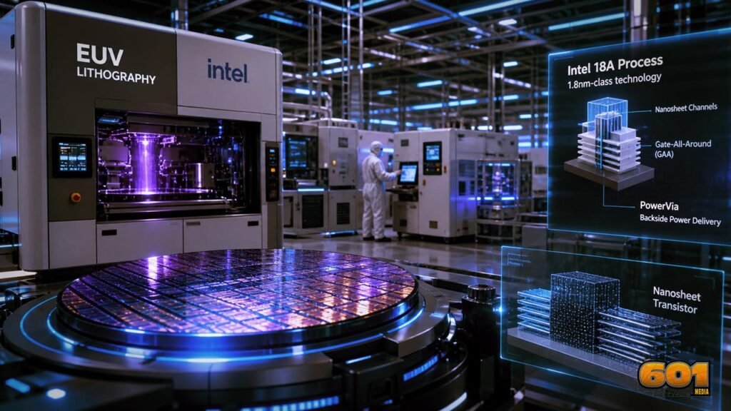
The 1.8nm-Class Semiconductor Technology Intel 18A is a major semiconductor process node built around RibbonFET gate-all-around transistors and PowerVia backside power delivery. It represents Intel’s attempt to regain process leadership and compete directly with TSMC and Samsung in the sub-2nm era. Table of contents What Is Intel 18A? Why Intel 18A Matters RibbonFET: Intel’s Gate-All-Around

Intel 18A, The 1.8nm-Class Semiconductor Read More »

In House Data Recovery

In-House Data Recovery

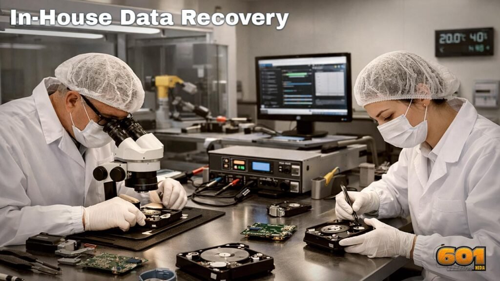
In-House Data Recovery: A Strategic Advantage for Modern Enterprises In-house data recovery refers to an organization’s ability to diagnose, repair, and restore lost or corrupted data using internal resources rather than relying on external service providers. As data volumes expand and operational dependence on digital systems deepens, this capability is no longer optional. It has

In-House Data Recovery Read More »

Sub-1nm Chip Fabrication

Sub-1nm Chip Fabrication Methods Explained

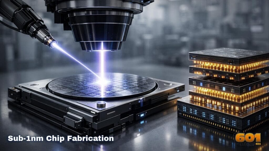
Sub-1nm Chip Fabrication Methods Explained Sub-1nm chip fabrication represents the most extreme frontier of semiconductor manufacturing, where innovation shifts from traditional scaling to atomic-level engineering, novel materials, and three-dimensional architectures to sustain performance gains beyond Moore’s Law. Table of Contents Why Sub-1nm Is a Fundamental Challenge Advanced Lithography Beyond EUV New Channel Materials at the

Sub-1nm Chip Fabrication Methods Explained Read More »

Next-Generation-Lithography-Technology-illustrated

Next-Generation Lithography Technology and the Future of Semiconductors

Next-Generation Lithography Technology and the Future of Semiconductors The semiconductor industry is approaching physical limits that once seemed theoretical. As transistors shrink below five nanometers, traditional lithography methods struggle to maintain precision, yield, and cost efficiency. Next-generation lithography technology is the defining factor that will determine how far Moore’s Law can continue, shaping the future

Next-Generation Lithography Technology and the Future of Semiconductors Read More »

X-ray-Lithography-in-Semiconductor-Manufacturing-illustrated

X-ray Lithography in Semiconductor Manufacturing Explained

X-ray Lithography in Semiconductor Manufacturing Explained X-ray lithography has long been viewed as one of the most technically ambitious approaches to semiconductor patterning. As transistor dimensions push beyond the limits of extreme ultraviolet lithography, X-ray lithography is re-emerging as a potential pathway to sustain Moore’s Law in the sub-5 nanometer era. Table of Contents What

X-ray Lithography in Semiconductor Manufacturing Explained Read More »

X-ray Lithography vs EUV Lithography

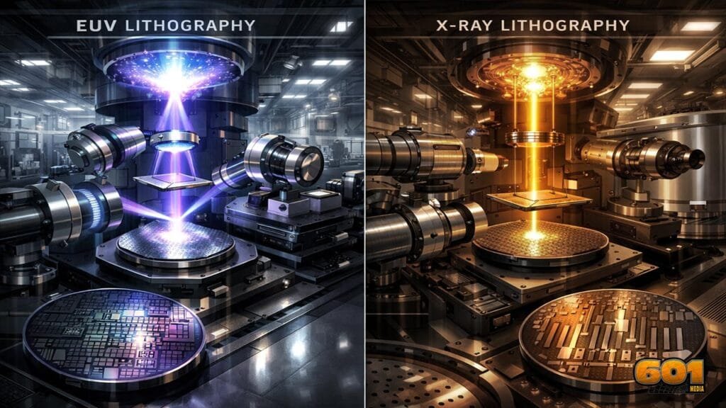
X-ray Lithography vs EUV Lithography

X-ray Lithography vs EUV Lithography: Key Differences and Industry Impact Manufacturing Modern semiconductor manufacturing is defined by how precisely engineers can pattern features measured in nanometers. As transistor sizes shrink and chip complexity explodes, lithography has become the primary bottleneck—and the primary differentiator—in advanced fabrication. Two technologies often compared in this context are X-ray lithography

X-ray Lithography vs EUV Lithography Read More »

X-ray Lithography

How X-ray Lithography Could Transform Chip Manufacturing

How X-ray Lithography Could Transform Chip Manufacturing. X-ray lithography has long been discussed as a breakthrough alternative to extreme ultraviolet lithography. As semiconductor scaling approaches physical and economic limits, this technology is re-emerging as a potential way to redefine how advanced chips are designed, patterned, and manufactured in the coming decades. TABLE OF CONTENTS The

How X-ray Lithography Could Transform Chip Manufacturing Read More »

AI-chip-sales-performance-illustration

AI Chip Sales Performance

AI Chip Sales Performance: A Data-Driven Overview of Market Growth, Leaders, and Future Trajectory AI chip sales have emerged as one of the strongest indicators of technological momentum in the global digital economy. As artificial intelligence moves from experimentation to large-scale deployment, demand for specialized computing hardware has surged. Using estimates from the Epoch AI

AI Chip Sales Performance Read More »

Pin It on Pinterest