The 1.8nm-Class Semiconductor Technology
Intel 18A is a major semiconductor process node built around RibbonFET gate-all-around transistors and PowerVia backside power delivery. It represents Intel’s attempt to regain process leadership and compete directly with TSMC and Samsung in the sub-2nm era.
Table of contents
- What Is Intel 18A?
- Why Intel 18A Matters
- RibbonFET: Intel’s Gate-All-Around Transistor
- PowerVia: Backside Power Delivery
- Performance and Efficiency Expectations
- Intel 18A vs TSMC and Samsung
- Key Applications
- Challenges and Risks
- Top 5 Frequently Asked Questions
- Final Thoughts
- Resources
What Is Intel 18A?
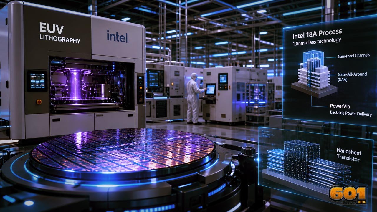
Intel 18A is Intel’s advanced semiconductor manufacturing process designed for the angstrom era. The “A” stands for angstrom, a unit equal to one-tenth of a nanometer. In simple terms, Intel 18A is commonly described as a 1.8nm-class node.
That does not mean every feature on the chip is literally 1.8 nanometers wide. Modern node names are no longer direct measurements of transistor gate length or metal pitch. Instead, they represent a technology generation that combines transistor scaling, density improvements, power efficiency, and manufacturing capability.
Intel 18A is important because it introduces two major innovations together: RibbonFET and PowerVia. RibbonFET changes the transistor structure, while PowerVia changes how power is delivered across the chip.
Why Intel 18A Matters
For decades, semiconductor progress depended on making transistors smaller. Smaller transistors allowed chipmakers to place more logic into the same silicon area, improving performance and reducing energy per operation.
That traditional scaling model has become harder. As transistors shrink, chip designers face leakage, heat, voltage loss, signal routing congestion, and rising manufacturing cost. Intel 18A addresses these problems by changing both the transistor and the power delivery architecture.
This matters far beyond Intel. Advanced process nodes support artificial intelligence, data centers, cloud infrastructure, edge devices, autonomous systems, and high-performance consumer electronics. More efficient chips can reduce energy consumption while enabling more compute-heavy workloads.
RibbonFET: Intel’s Gate-All-Around Transistor
RibbonFET is Intel’s gate-all-around transistor architecture. It replaces the FinFET structure that has powered many previous generations of advanced chips.
In a FinFET, the gate wraps around three sides of a fin-shaped channel. In a gate-all-around design, the gate surrounds the channel more completely. Intel’s RibbonFET uses stacked nanosheet-like channels, giving the gate stronger control over current flow.
The main benefit is better electrostatic control. That means the transistor can switch more cleanly, leak less current, and operate efficiently at smaller dimensions. For chip designers, this can translate into higher performance, lower power use, or a better balance of both.
PowerVia: Backside Power Delivery
PowerVia is Intel’s backside power delivery technology. Traditional chips route both power and signals through the front side of the wafer. As chips become denser, that front-side routing becomes crowded.
PowerVia separates power delivery from signal routing by moving power lines to the backside of the silicon. This gives signal wires more room on the front side and allows power to reach transistors more directly.
The result can include reduced voltage droop, improved routing efficiency, and better performance under demanding workloads. In practical terms, PowerVia helps the chip maintain stable power delivery when billions of transistors switch rapidly.
Performance and Efficiency Expectations
Intel has positioned 18A as a major step for performance-per-watt. Performance-per-watt is especially important because modern computing is limited not only by speed, but also by heat and energy cost.
For artificial intelligence and data center processors, energy efficiency directly affects operating cost. A chip that delivers more work per watt can reduce cooling demand, improve server density, and lower total cost of ownership.
For consumer devices, the same principle improves battery life and thermal behavior. Faster chips matter, but cooler and more efficient chips often matter just as much.
Intel 18A vs TSMC and Samsung
Intel 18A enters a highly competitive market. TSMC and Samsung are also developing advanced gate-all-around and sub-2nm-class manufacturing technologies.
TSMC remains the dominant pure-play foundry, serving major customers across mobile, AI, graphics, and high-performance computing. Samsung has also invested heavily in gate-all-around technology and advanced foundry services.
Intel’s strategy is different because it is both a chip designer and a manufacturer. Through Intel Foundry, the company wants to manufacture chips not only for itself but also for external customers. If Intel 18A performs well in yield, cost, and reliability, it could become a serious alternative for companies seeking advanced-node supply diversification.
Key Applications
Intel 18A can support several high-value markets. In artificial intelligence, more efficient transistors can help accelerate model training and inference. In data centers, better power efficiency can reduce infrastructure costs. In personal computing, advanced process technology can improve performance while supporting thinner and quieter systems.
Automotive and edge computing may also benefit. Vehicles, industrial equipment, and connected devices increasingly need local compute power for sensing, decision-making, and security. Efficient advanced chips can support these workloads without excessive heat or energy draw.
Challenges and Risks
Intel 18A is ambitious, and ambition brings execution risk. Gate-all-around transistors are more complex to manufacture than FinFETs. Backside power delivery also changes process integration, design rules, testing, and yield learning.
Yield is one of the most important challenges. A process node can look impressive on paper, but it must produce usable chips at commercial scale. If yields are low, costs rise and customers hesitate.
Intel must also prove that its foundry ecosystem can support external customers. Advanced manufacturing is not only about transistors. It also requires design tools, IP libraries, packaging options, customer support, and predictable delivery.
Top 5 Frequently Asked Questions
Final Thoughts
The most important takeaway is that Intel 18A is not just another node shrink. It represents a broader shift in semiconductor innovation. The industry can no longer rely only on making transistors smaller. Future gains will come from better transistor structures, smarter power delivery, advanced packaging, and stronger manufacturing ecosystems.
Intel 18A matters because it combines two major architectural changes at once. RibbonFET improves how transistors switch. PowerVia improves how power reaches them. If Intel executes well, 18A could strengthen its position in advanced manufacturing and give the global semiconductor market another competitive leading-edge foundry option.
Resources
- Intel Technology Roadmaps and Milestones
- Intel Foundry Press Kit
- Intel Process and Packaging Innovations
- IEEE Spectrum coverage of Intel 18A
- TSMC 2nm Technology Overview
- Samsung Foundry Gate-All-Around Technology
I am a huge enthusiast for Computers, AI, SEO-SEM, VFX, and Digital Audio-Graphics-Video. I’m a digital entrepreneur since 1992. Articles include AI assisted research. Always Keep Learning! Notice: All content is published for educational and entertainment purposes only. NOT LIFE, HEALTH, SURVIVAL, FINANCIAL, BUSINESS, LEGAL OR ANY OTHER ADVICE. Learn more about Mark Mayo