X-ray Lithography vs EUV Lithography: Key Differences and Industry Impact Manufacturing
Modern semiconductor manufacturing is defined by how precisely engineers can pattern features measured in nanometers. As transistor sizes shrink and chip complexity explodes, lithography has become the primary bottleneck—and the primary differentiator—in advanced fabrication. Two technologies often compared in this context are X-ray lithography and extreme ultraviolet (EUV) lithography. While both aim to overcome the limits of traditional optical lithography, only one has achieved large-scale industrial adoption. This article explains how these technologies work, why EUV won the race, and whether X-ray lithography still has a future.
TABLE OF CONTENTS
- Lithography Basics in Semiconductor Manufacturing
- What Is X-ray Lithography?
- What Is EUV Lithography?
- Technical Comparison: X-ray vs EUV
- Manufacturing and Economic Realities
- Industry Adoption and Ecosystem Support
- Future Outlook for Both Technologies
- Top 5 Frequently Asked Questions
- Final Thoughts
- Resources
Lithography Basics in Semiconductor Manufacturing
Lithography is the process of transferring circuit patterns from a mask onto a silicon wafer using light or radiation. Resolution depends primarily on wavelength: shorter wavelengths enable smaller features. Traditional deep ultraviolet lithography, using 193 nm light, reached its physical limits years ago. To continue scaling, the industry explored radically shorter wavelengths, including X-rays and extreme ultraviolet light. At sub-10 nm nodes, lithography determines not only feature size but yield, power efficiency, and cost per transistor. This makes the choice of lithography technology a strategic decision with multi-billion-dollar consequences.
What Is X-ray Lithography?
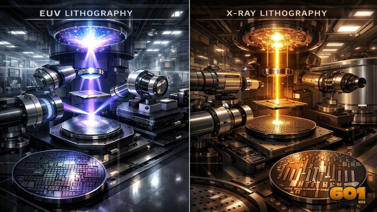
X-ray lithography uses soft X-rays with wavelengths typically between 0.1 and 10 nanometers. In theory, this enables extremely high resolution, well below what EUV can achieve. The process relies on proximity printing, where a mask is placed very close to the wafer without direct contact. X-ray lithography attracted strong research interest in the 1980s and 1990s, particularly for its potential to bypass optical diffraction limits entirely. Early demonstrations showed impressive resolution, even by today’s standards. However, the technology faced major obstacles. X-ray masks are extraordinarily difficult to fabricate and align. Suitable resists were slow and fragile. Most critically, high-power, reliable X-ray sources proved impractical for high-volume manufacturing. As a result, X-ray lithography remained confined to laboratories and niche research environments rather than commercial fabs.
What Is EUV Lithography?
EUV lithography uses 13.5 nm wavelength light—short enough to enable patterning at 5 nm nodes and beyond. Unlike X-ray lithography, EUV uses reflective optics instead of lenses because EUV light is absorbed by nearly all materials. The EUV system is one of the most complex machines ever built. It requires a vacuum environment, ultra-flat mirrors with atomic-level precision, and a plasma-based light source generated by firing lasers at molten tin droplets. Despite its complexity, EUV succeeded where X-ray lithography failed: it scaled into high-volume manufacturing. Today, EUV is the backbone of advanced logic production at leading-edge nodes.
Technical Comparison: X-ray vs EUV
From a purely physical standpoint, X-ray lithography offers superior theoretical resolution. Shorter wavelengths reduce diffraction and enable smaller features. However, lithography is not just about wavelength—it is about system integration. EUV lithography strikes a balance between resolution, throughput, and control. While its wavelength is longer than X-rays, advanced techniques such as multiple patterning, stochastic defect mitigation, and computational lithography compensate for this limitation. X-ray lithography struggles with mask distortion, thermal expansion, and alignment accuracy. EUV masks, though challenging, benefit from decades of optical metrology and precision engineering expertise. In practice, EUV delivers usable resolution at industrial speeds. X-ray lithography does not.
Manufacturing and Economic Realities
Manufacturing economics ultimately determine technology adoption. EUV systems cost over $150 million per tool, yet they still make financial sense because they replace multiple deep ultraviolet patterning steps. X-ray lithography, by contrast, would require entirely new infrastructure, mask ecosystems, and defect inspection technologies. The cost and risk are prohibitive without a clear performance advantage over EUV. Additionally, EUV benefits from a mature supplier network and massive R&D investment, particularly from ASML, which has spent more than two decades refining EUV systems.
Industry Adoption and Ecosystem Support
EUV lithography is used in high-volume manufacturing by leading chipmakers including TSMC, Samsung, and Intel. Entire process flows, from design rules to yield optimization, are built around EUV. X-ray lithography lacks this ecosystem. Without industry-wide adoption, supporting technologies such as inspection tools, resists, and repair systems never reached maturity. In semiconductor manufacturing, ecosystem momentum is often more important than theoretical superiority. EUV achieved critical mass; X-ray lithography did not.
Future Outlook for Both Technologies
EUV lithography will remain dominant through the remainder of the decade. High-NA EUV, with numerical apertures above 0.5, is already being deployed to extend scaling toward 2 nm and beyond. X-ray lithography may still find relevance in niche applications such as advanced research, nanofabrication for scientific instruments, or specialized photonics. However, it is unlikely to re-enter mainstream semiconductor manufacturing. The lesson is clear: technological viability depends not only on physics, but on manufacturability, economics, and ecosystem alignment.
Top 5 Frequently Asked Questions
Final Thoughts
EUV lithography didn’t “win” because it was the shortest wavelength option on the table—it won because it was the first next-generation approach that could be engineered into a repeatable, high-throughput manufacturing system with a scalable supply chain. That distinction matters. In semiconductor production, the best technology is the one that can deliver nanometer precision at industrial speed, with predictable yield, inspectability, and cost control across millions of wafers.
X-ray lithography remains a powerful idea in physics terms. Its wavelength range is inherently capable of finer patterning than EUV, and that has kept it relevant in research and specialized nanofabrication contexts. But the same attributes that make X-rays attractive—strong absorption in materials, difficult mask mechanics, and strict source requirements—also make them exceptionally hard to productize for high-volume logic fabs. In other words, X-ray lithography is a “resolution-first” solution in a world where the problem is “manufacturing-first.”
EUV, meanwhile, represents a systems-engineering triumph. It turned a fundamentally hostile wavelength—absorbed by air, blocked by glass, and intolerant of contamination—into a production platform by building an entire environment around it: vacuum tool architecture, reflective optics, mask infrastructure, contamination control, defect inspection, and computational patterning. That ecosystem is now so mature that the industry’s roadmap extends EUV forward with high-NA systems, rather than switching paradigms again.
The most important takeaway is this: lithography decisions are rarely settled by theoretical limits alone. They’re settled by the ability to integrate optics, materials, metrology, tooling, and economics into a reliable manufacturing loop. EUV achieved that integration. X-ray lithography never crossed that threshold. Unless a new breakthrough dramatically changes X-ray sources, mask technologies, and inspection—at a cost that beats the EUV + high-NA trajectory—EUV will remain the foundation of leading-edge semiconductor scaling for the foreseeable future.
I am a huge enthusiast for Computers, AI, SEO-SEM, VFX, and Digital Audio-Graphics-Video. I’m a digital entrepreneur since 1992. Articles include AI assisted research. Always Keep Learning! Notice: All content is published for educational and entertainment purposes only. NOT LIFE, HEALTH, SURVIVAL, FINANCIAL, BUSINESS, LEGAL OR ANY OTHER ADVICE. Learn more about Mark Mayo