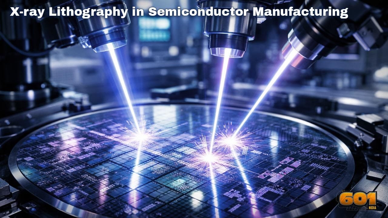
X-ray Lithography in Semiconductor Manufacturing Explained
X-ray lithography has long been viewed as one of the most technically ambitious approaches to semiconductor patterning. As transistor dimensions push beyond the limits of extreme ultraviolet lithography, X-ray lithography is re-emerging as a potential pathway to sustain Moore’s Law in the sub-5 nanometer era.
Table of Contents
- What Is X-ray Lithography?
- Why Traditional Lithography Is Reaching Its Limits
- How X-ray Lithography Works
- Technical Advantages of X-ray Lithography
- Key Challenges and Barriers to Adoption
- Comparison With EUV Lithography
- Current Research and Industry Progress
- Future Outlook for X-ray Lithography
- Top 5 Frequently Asked Questions
- Final Thoughts
- Resources
What Is X-ray Lithography?
X-ray lithography is a semiconductor manufacturing technique that uses short-wavelength X-rays, typically in the 0.1 to 10 nanometer range, to transfer circuit patterns onto silicon wafers. The shorter wavelength enables significantly higher resolution than optical and deep ultraviolet lithography. Unlike projection-based systems, X-ray lithography relies on proximity printing. A mask containing the circuit pattern is positioned extremely close to the wafer, allowing X-rays to expose a resist layer with minimal diffraction.
Why Traditional Lithography Is Reaching Its Limits
Deep ultraviolet lithography plateaued below 40 nanometers due to diffraction limits. Extreme ultraviolet lithography extended scaling to 5 nanometers and below, but at enormous cost and complexity. EUV systems require ultra-high vacuum, reflective optics with atomic-level precision, and light sources delivering over 250 watts of power. Yield sensitivity and escalating capital expenditures are forcing the industry to explore alternatives that can deliver finer resolution without exponential cost increases.
How X-ray Lithography Works
X-ray lithography begins with a high-energy X-ray source, often a synchrotron or plasma-based emitter. The X-rays pass through a membrane-based mask, typically composed of low-atomic-number materials like silicon nitride. The exposed photoresist undergoes chemical changes, allowing selective removal during development. Because X-rays exhibit negligible diffraction at nanometer scales, feature sizes below 2 nanometers are theoretically achievable.
Technical Advantages of X-ray Lithography
The most compelling advantage of X-ray lithography is resolution. The physics of shorter wavelengths directly translate into finer pattern fidelity and reduced line edge roughness. Depth of focus is also significantly improved, enabling better pattern transfer across wafer topography. Additionally, X-ray lithography avoids the multilayer reflective optics required by EUV, simplifying optical system design.
Key Challenges and Barriers to Adoption
Despite its promise, X-ray lithography faces formidable obstacles. Mask fabrication is exceptionally difficult due to the need for ultra-thin, defect-free membranes that can withstand radiation without distortion. X-ray sources are another major hurdle. Synchrotron facilities are impractical for high-volume manufacturing, while compact plasma sources still struggle with efficiency, stability, and cost. Resist sensitivity also remains a concern. Many existing photoresists exhibit poor absorption at X-ray wavelengths, leading to low throughput and increased exposure times.
Comparison With EUV Lithography
EUV lithography dominates current leading-edge production, but its complexity is unmatched. EUV relies on multilayer Bragg reflectors with over 100 precision-coated layers, each defect potentially impacting yield. X-ray lithography eliminates reflective optics altogether. However, EUV benefits from decades of industrial investment, while X-ray lithography remains largely confined to research environments. From a cost perspective, X-ray lithography could ultimately be more scalable if compact, efficient sources are commercialized.
Current Research and Industry Progress
National laboratories and academic institutions are actively revisiting X-ray lithography using modern materials science and nanofabrication techniques. Advances in graphene membranes, metal-oxide resists, and laser-driven plasma sources are reshaping feasibility assumptions. Research published in Applied Physics Letters and IEEE journals demonstrates sub-2 nanometer patterning with acceptable line roughness, reigniting industrial interest.
Future Outlook for X-ray Lithography
X-ray lithography is unlikely to replace EUV in the short term. Instead, it may emerge as a complementary or niche solution for advanced logic, memory, and quantum devices. If scalable X-ray sources and robust mask technologies mature, X-ray lithography could become a cornerstone technology for post-silicon scaling strategies beyond 2030.
Top 5 Frequently Asked Questions
Final Thoughts
X-ray lithography represents a powerful yet underutilized tool in semiconductor manufacturing. Its ability to transcend diffraction limits positions it as a potential successor technology in a post-EUV world. While technical and economic barriers remain, ongoing research continues to narrow the gap between laboratory success and industrial reality.
Resources
- IEEE Transactions on Semiconductor Manufacturing
- Applied Physics Letters – X-ray Nanopatterning Studies
- International Roadmap for Devices and Systems (IRDS)
- MIT Lincoln Laboratory Nanofabrication Research
I am a huge enthusiast for Computers, AI, SEO-SEM, VFX, and Digital Audio-Graphics-Video. I’m a digital entrepreneur since 1992. Articles include AI assisted research. Always Keep Learning! Notice: All content is published for educational and entertainment purposes only. NOT LIFE, HEALTH, SURVIVAL, FINANCIAL, BUSINESS, LEGAL OR ANY OTHER ADVICE. Learn more about Mark Mayo