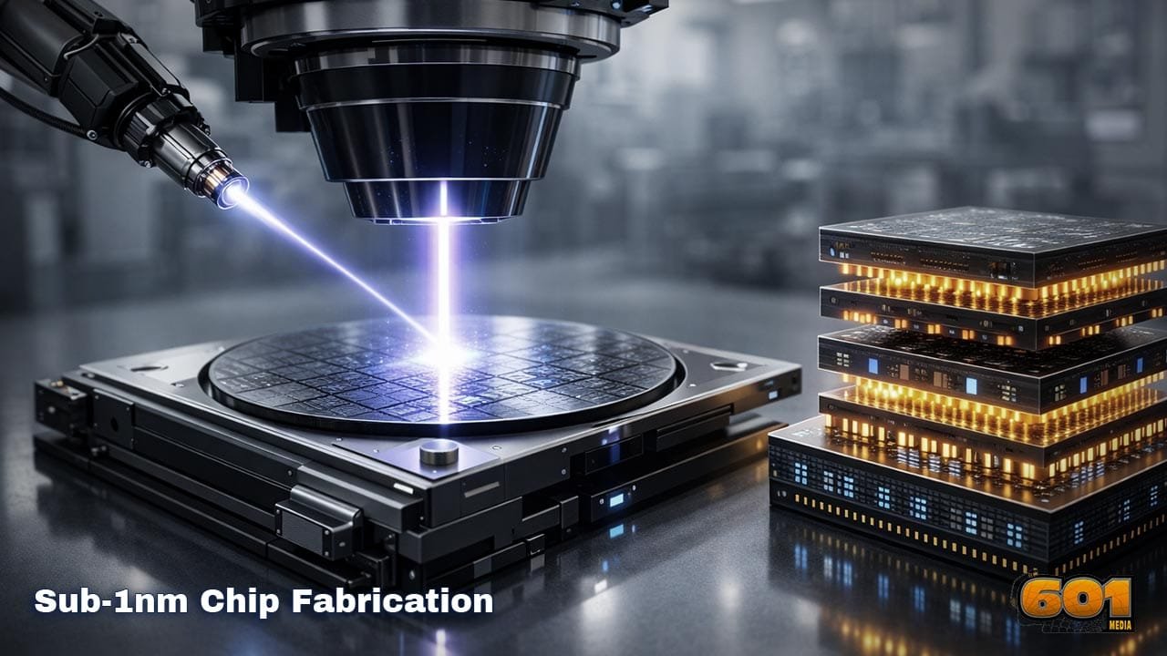
Sub-1nm Chip Fabrication Methods Explained
Sub-1nm chip fabrication represents the most extreme frontier of semiconductor manufacturing, where innovation shifts from traditional scaling to atomic-level engineering, novel materials, and three-dimensional architectures to sustain performance gains beyond Moore’s Law.
Table of Contents
- Why Sub-1nm Is a Fundamental Challenge
- Advanced Lithography Beyond EUV
- New Channel Materials at the Atomic Scale
- Gate-All-Around and CFET Transistor Architectures
- Atomic-Scale Manufacturing Techniques
- 3D Integration and Advanced Packaging
- Economic and Yield Constraints
- Industry Roadmaps and Timelines
- Top 5 Frequently Asked Questions
- Final Thoughts
- Resources
Why Sub-1nm Is a Fundamental Challenge
Sub-1nm nodes operate at dimensions smaller than the width of five silicon atoms, where classical semiconductor physics no longer applies cleanly. At this scale, quantum tunneling causes electrons to leak through transistor gates, variability increases due to single-atom defects, and thermal dissipation becomes a dominant bottleneck. Traditional Dennard scaling broke down long ago, and even Moore’s Law now depends more on architectural ingenuity than raw transistor density. Process variation at sub-1nm means that statistical averages are insufficient. Each transistor behaves slightly differently, forcing designers to co-optimize devices, circuits, and software. According to IEEE studies, line-edge roughness of just 0.3 nm can reduce yield by over 20 percent at these dimensions.
Advanced Lithography Beyond EUV
Extreme ultraviolet lithography at a 13.5 nm wavelength enabled 5 nm and 3 nm nodes, largely driven by ASML. Sub-1nm, however, pushes EUV to its physical resolution limit. High-NA EUV systems with numerical apertures of 0.55 improve resolution but introduce depth-of-focus challenges and tighter overlay tolerances. Multi-patterning returns as a necessity, increasing cost and defect risk. Research into soft X-ray lithography and directed self-assembly is ongoing, but neither is production-ready. In practice, sub-1nm patterning relies on a hybrid approach: EUV defines coarse features while atomic-level deposition and etching finalize critical dimensions.
New Channel Materials at the Atomic Scale
Silicon channels cannot maintain electrostatic control below roughly 2 nm gate lengths. The industry is transitioning to alternative materials with higher carrier mobility and better confinement. Two-dimensional materials such as molybdenum disulfide and tungsten diselenide offer atomically thin channels that suppress short-channel effects. Carbon nanotubes provide ballistic transport properties, with experimental devices demonstrating near-ideal switching behavior at sub-1nm equivalent lengths. However, integrating these materials into CMOS-compatible processes remains a major obstacle. Contact resistance, large-scale uniformity, and contamination control are still unresolved at manufacturing scale.
Gate-All-Around and CFET Transistor Architectures
Gate-all-around nanosheet transistors are the last evolutionary step of planar silicon devices. They fully surround the channel, restoring electrostatic control lost at smaller nodes. Below 1 nm, even GAA reaches its limits. The next step is complementary FETs, or CFETs, which vertically stack n-type and p-type transistors. This approach doubles device density without shrinking lateral dimensions. TSMC and Samsung Electronics have both published CFET roadmaps targeting the early 2030s. CFETs introduce extreme process complexity, requiring atomic-level alignment and defect-free interlayer connections.
Atomic-Scale Manufacturing Techniques
Sub-1nm fabrication depends less on lithography and more on precision material control. Atomic layer deposition enables monolayer-thick films with angstrom-level uniformity. Atomic layer etching removes material one atomic plane at a time, reducing line-edge roughness. Selective deposition techniques eliminate the need for some lithography steps entirely by growing materials only where needed. These methods reduce variability and improve yield but demand unprecedented contamination control and metrology resolution. Process control now relies on in-line electron microscopy and AI-driven defect classification to manage atomic-scale variation.
3D Integration and Advanced Packaging
As transistor scaling slows, performance gains increasingly come from three-dimensional integration. Chiplets, through-silicon vias, and hybrid bonding enable higher bandwidth and lower latency without shrinking transistors further. Logic-on-logic stacking allows memory and compute elements to sit microns apart, dramatically reducing interconnect energy. This approach shifts innovation from front-end fabrication to back-end assembly, extending performance scaling even when transistor density plateaus.
Economic and Yield Constraints
Sub-1nm fabs are projected to exceed 30 billion USD per facility, with EUV tools alone costing over 350 million USD each. Yield losses from atomic-scale defects mean that only a handful of companies can afford to compete. This economic pressure accelerates industry consolidation and increases reliance on government subsidies. It also forces design teams to prioritize system-level optimization over raw transistor counts.
Industry Roadmaps and Timelines
Industry consensus suggests that true sub-1nm production will appear between 2030 and 2035, initially for high-performance computing and AI accelerators. IEEE roadmaps emphasize heterogeneous integration and energy efficiency over continued geometric scaling. Rather than a single breakthrough, sub-1nm will emerge as a convergence of materials science, device physics, and manufacturing automation.
Top 5 Frequently Asked Questions
Final Thoughts
Sub-1nm chip fabrication is less about shrinking transistors and more about redefining how computation is built. Atomic precision, novel materials, vertical integration, and economic realism now define progress. The most important takeaway is that innovation has shifted from geometry to systems engineering, where success depends on orchestrating physics, manufacturing, and architecture as a unified discipline.
Resources
- IEEE International Roadmap for Devices and Systems
- ASML High-NA EUV Technical Papers
- Nature Electronics: 2D Materials for CMOS
- IMEC Sub-1nm Research Publications
I am a huge enthusiast for Computers, AI, SEO-SEM, VFX, and Digital Audio-Graphics-Video. I’m a digital entrepreneur since 1992. Articles include AI assisted research. Always Keep Learning! Notice: All content is published for educational and entertainment purposes only. NOT LIFE, HEALTH, SURVIVAL, FINANCIAL, BUSINESS, LEGAL OR ANY OTHER ADVICE. Learn more about Mark Mayo