Next-Generation Lithography Technology and the Future of Semiconductors
The semiconductor industry is approaching physical limits that once seemed theoretical. As transistors shrink below five nanometers, traditional lithography methods struggle to maintain precision, yield, and cost efficiency. Next-generation lithography technology is the defining factor that will determine how far Moore’s Law can continue, shaping the future of artificial intelligence, high-performance computing, automotive electronics, and advanced communications.
TABLE OF CONTENTS
- The Evolution of Lithography in Semiconductor Manufacturing
- Extreme Ultraviolet Lithography (EUV): The Current Frontier
- What Defines Next-Generation Lithography?
- High-NA EUV: Pushing Beyond Today’s Limits
- Beyond EUV: Emerging Lithography Alternatives
- Cost, Yield, and the Business Impact
- Technical and Supply-Chain Challenges
- The Future Roadmap of Lithography Technology
- Top 5 Frequently Asked Questions
- Final Thoughts
- Resources
The Evolution of Lithography in Semiconductor Manufacturing
Lithography is the process of transferring circuit patterns onto silicon wafers. For decades, progress followed a predictable path: shorter wavelengths enabled smaller features. Deep ultraviolet (DUV) lithography dominated the industry through the 90-nanometer to 7-nanometer eras, supported by increasingly complex multi-patterning techniques. However, DUV reached a point of diminishing returns. Each additional patterning step increased defect rates, cycle time, and manufacturing cost. By the late 2010s, the industry required a fundamentally different approach rather than incremental optimization.
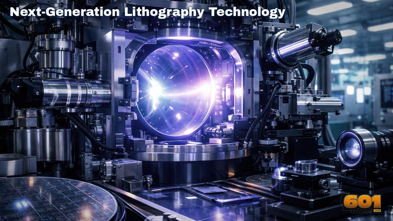
Extreme Ultraviolet Lithography (EUV): The Current Frontier
Extreme ultraviolet lithography uses a 13.5-nanometer wavelength, nearly an order of magnitude shorter than DUV. This enables single-exposure patterning for features previously requiring four or more DUV passes. ASML is currently the sole supplier of EUV lithography systems, with each machine costing over $150 million. Despite the cost, EUV adoption accelerated rapidly after 2019 due to its ability to improve yield and reduce process complexity at advanced nodes. Leading chipmakers such as TSMC and Samsung Electronics rely heavily on EUV for 5-nanometer and 3-nanometer production.
What Defines Next-Generation Lithography?
Next-generation lithography goes beyond simply reducing wavelength. It encompasses a combination of optical innovation, materials science, computational lithography, and system-level integration.
Key defining attributes include:
- Higher numerical aperture (NA) optics for improved resolution
- Advanced photoresists with reduced stochastic defects
- AI-driven process control and mask optimization
- Reduced pattern variability at atomic scales
From a technology management perspective, the shift is no longer just about equipment performance. It is about ecosystem coordination across suppliers, fabs, and design teams.
High-NA EUV: Pushing Beyond Today’s Limits
High-NA EUV is the most immediate evolution of current EUV systems. By increasing numerical aperture from 0.33 to 0.55, High-NA EUV enables tighter patterning for sub-2-nanometer nodes.
The trade-offs are significant:
- Smaller exposure fields requiring new chip layout strategies
- Higher sensitivity to vibration and alignment errors
- Even higher capital expenditure per tool
Despite these challenges, High-NA EUV is widely viewed as essential for sustaining logic scaling through the end of this decade.
Beyond EUV: Emerging Lithography Alternatives
While EUV dominates current roadmaps, research continues into alternative lithography approaches that could supplement or disrupt the existing paradigm. Directed self-assembly (DSA) leverages chemical properties of block copolymers to form extremely small, regular patterns. Nanoimprint lithography physically stamps patterns onto wafers, offering high resolution with lower equipment cost, though defect control remains a concern. These technologies are unlikely to replace EUV for leading-edge logic but may play critical roles in memory, specialty chips, and advanced packaging.
Cost, Yield, and the Business Impact
Next-generation lithography fundamentally reshapes semiconductor economics. Tool costs rise sharply, but fewer process steps and improved yield offset some of the capital burden. For foundries, the strategic implication is clear: only companies with massive scale and long-term customer commitments can justify continued investment. This reinforces industry consolidation and raises barriers to entry for new competitors. From an innovation management lens, lithography has become both a technical bottleneck and a competitive moat.
Technical and Supply-Chain Challenges
Next-generation lithography faces persistent challenges:
- Stochastic defects caused by photon shot noise
- Limited availability of EUV-compatible materials
- Highly concentrated supplier ecosystems
Supply-chain resilience is now a strategic priority, not an operational concern. Any disruption in optics, light sources, or photoresists can halt multi-billion-dollar fabs.
The Future Roadmap of Lithography Technology
The future of lithography will be hybrid rather than singular. EUV, High-NA EUV, advanced DUV, and complementary patterning methods will coexist, optimized for specific layers and applications. Longer term, innovation may shift from purely optical scaling to system-level efficiency, including chiplet architectures and 3D integration, reducing reliance on extreme lithographic precision alone.
Top 5 Frequently Asked Questions
Final Thoughts
Next-generation lithography technology is not just a manufacturing upgrade. It is the strategic foundation of modern digital infrastructure. As physical limits tighten, innovation shifts from incremental improvements to coordinated breakthroughs across optics, materials, software, and organizational capability. Companies that master this transition will define the next decade of technological leadership.
Resources
- ASML Technology Overview
- IEEE Spectrum: EUV Lithography Reports
- International Roadmap for Devices and Systems (IRDS)
I am a huge enthusiast for Computers, AI, SEO-SEM, VFX, and Digital Audio-Graphics-Video. I’m a digital entrepreneur since 1992. Articles include AI assisted research. Always Keep Learning! Notice: All content is published for educational and entertainment purposes only. NOT LIFE, HEALTH, SURVIVAL, FINANCIAL, BUSINESS, LEGAL OR ANY OTHER ADVICE. Learn more about Mark Mayo