How X-ray Lithography Could Transform Chip Manufacturing.
X-ray lithography has long been discussed as a breakthrough alternative to extreme ultraviolet lithography. As semiconductor scaling approaches physical and economic limits, this technology is re-emerging as a potential way to redefine how advanced chips are designed, patterned, and manufactured in the coming decades.
TABLE OF CONTENTS
- The Scaling Crisis in Modern Chip Manufacturing
- What X-ray Lithography Is and How It Works
- X-ray Lithography vs EUV Lithography
- How X-ray Lithography Could Reshape Manufacturing
- Economic and Strategic Implications
- Key Technical and Commercial Barriers
- Adoption Timelines and Industry Outlook
- Top 5 Frequently Asked Questions
- Final Thoughts
- Resources
The Scaling Crisis in Modern Chip Manufacturing
For over five decades, the semiconductor industry has relied on lithographic scaling to deliver denser, faster, and more energy-efficient chips. That model is under pressure. Transistor feature sizes below 5 nanometers demand extreme precision, tighter process control, and exponentially higher capital investment. The cost of a leading-edge fabrication facility now exceeds 20 billion dollars, while yield optimization becomes increasingly fragile. Extreme ultraviolet lithography enabled the 7 nm, 5 nm, and early 3 nm nodes, but it is reaching a point of diminishing returns. Optical constraints, mask complexity, stochastic defects, and multi-patterning requirements introduce variability that directly impacts yield and reliability. These constraints are not theoretical. They are already shaping roadmaps, delaying node transitions, and forcing chipmakers to rethink scaling strategies.
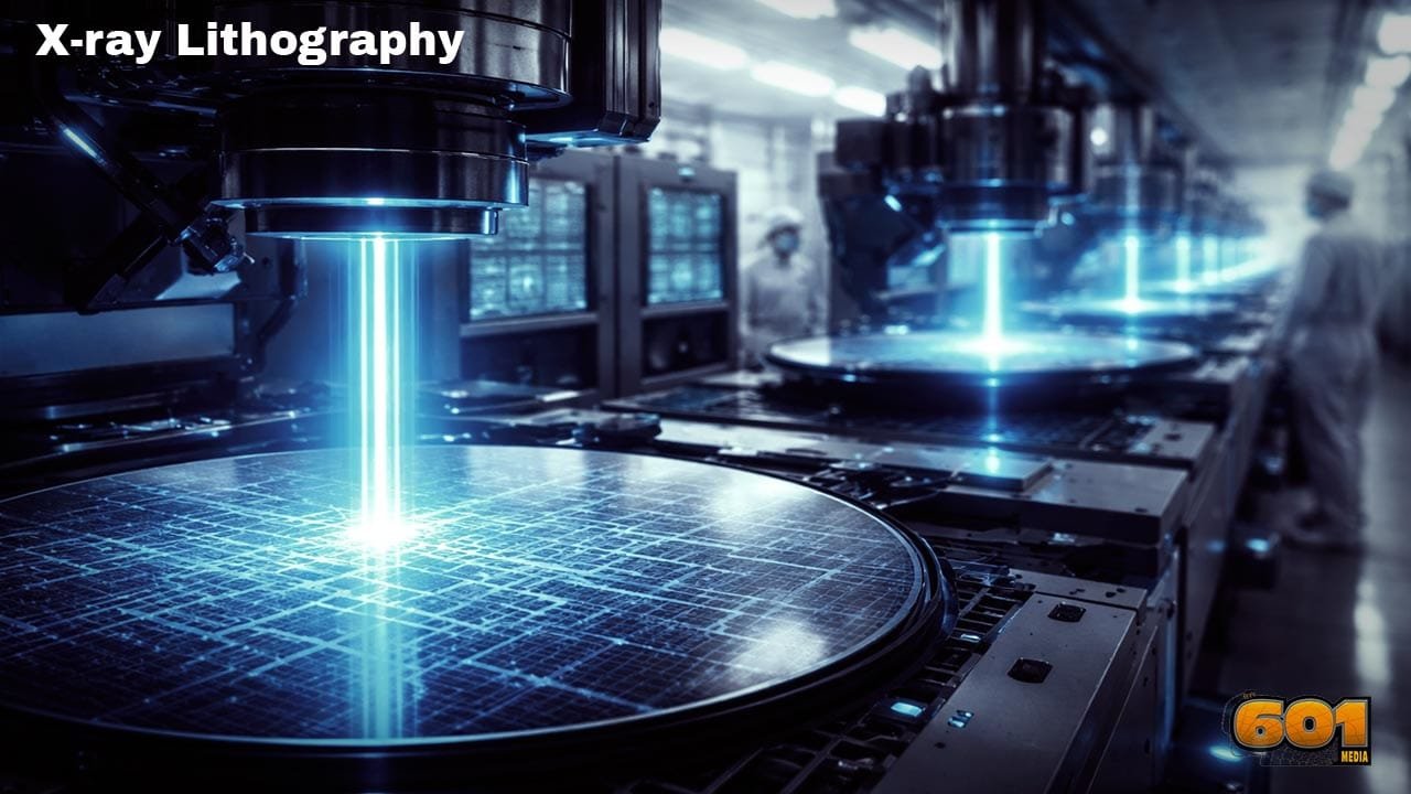
What X-ray Lithography Is and How It Works
X-ray lithography uses significantly shorter wavelengths than deep ultraviolet or extreme ultraviolet systems. While EUV operates at 13.5 nanometers, X-ray lithography works at wavelengths below 1 nanometer. This reduction dramatically improves theoretical resolution and depth of focus, enabling far finer patterning with less optical distortion. Instead of refractive or reflective optics, X-ray lithography relies on proximity printing or advanced projection systems using specialized mirrors and masks. High-energy X-rays penetrate resist materials differently, reducing diffraction effects and enabling sharper feature edges. In practical terms, this means the ability to define denser patterns with fewer process steps. Recent advances in synchrotron radiation sources, compact X-ray generators, and resist chemistry have revived interest in this approach. What once required massive research facilities is slowly moving toward industrial feasibility.
X-ray Lithography vs EUV Lithography
The most immediate difference between X-ray lithography and EUV is resolution headroom. EUV is already operating near its physical wavelength limits. Any further scaling requires increasingly complex computational lithography and pattern correction techniques. X-ray lithography, by contrast, offers a new scaling runway. Another key distinction lies in pattern fidelity. X-rays exhibit reduced line edge roughness compared to EUV, which is increasingly affected by photon shot noise. This directly translates into more consistent transistor dimensions and improved electrical performance. However, EUV currently benefits from a mature ecosystem. Tool suppliers, resist vendors, and fabs have invested over a decade in optimization. X-ray lithography lacks this level of integration today, making near-term replacement unrealistic but long-term disruption plausible.
How X-ray Lithography Could Reshape Manufacturing
If successfully commercialized, X-ray lithography would simplify process flows at advanced nodes. Fewer multi-patterning steps reduce cycle time, lower defect density, and improve yield stability. This has direct implications for fab productivity and cost per wafer. Design rules would also evolve. Chip architects could rely on more predictable patterning, enabling tighter layouts and higher transistor densities without excessive design guardbands. This could slow the industry’s shift toward costly architectural workarounds such as chiplets and advanced packaging, restoring some benefits of monolithic scaling. From a manufacturing control perspective, higher process margins improve repeatability across wafers and lots. This is critical as artificial intelligence accelerators and high-performance computing chips demand consistent performance at scale.
Economic and Strategic Implications
X-ray lithography could significantly alter the economics of leading-edge manufacturing. While early tools would be expensive, reduced process complexity may lower long-term operating costs. Fewer patterning steps translate into lower energy usage, reduced consumables, and higher effective throughput. Strategically, this technology could rebalance industry power. Nations and companies that master X-ray lithography early may leapfrog existing EUV leaders. This has implications for supply chain resilience, national semiconductor strategies, and geopolitical competition in advanced manufacturing. For fabless companies, access to more predictable scaling could extend the life of traditional CMOS roadmaps, reducing pressure to adopt exotic materials or radical architectural changes prematurely.
Key Technical and Commercial Barriers
Despite its promise, X-ray lithography faces substantial obstacles. Mask fabrication remains extremely challenging due to the need for defect-free, radiation-resistant materials. Resist sensitivity must improve to enable acceptable throughput without compromising resolution. Tool reliability is another concern. X-ray sources must deliver stable, high-intensity radiation over long operating lifetimes. Any instability directly impacts yield and uptime, both critical in high-volume manufacturing. Finally, ecosystem readiness is a major hurdle. Design tools, metrology systems, and process control software must be rebuilt or heavily adapted. This transition requires coordination across suppliers, fabs, and designers, something the industry historically approaches cautiously.
Adoption Timelines and Industry Outlook
Most experts agree that X-ray lithography will not replace EUV in the immediate future. A realistic adoption window lies in the post-2 nm era, where conventional scaling approaches become economically unsustainable. Initial deployment is likely in research fabs or specialized high-value applications before broader adoption. Over the next decade, hybrid approaches may emerge, combining EUV for certain layers with X-ray lithography for the most critical features. This incremental integration would reduce risk while validating performance at scale.
Top 5 Frequently Asked Questions
Final Thoughts
X-ray lithography represents more than an incremental improvement. It offers a potential reset for semiconductor scaling at a time when existing approaches are straining under physical and economic limits. While formidable challenges remain, the strategic value of renewed scaling headroom is immense. If the industry succeeds in translating laboratory progress into manufacturing reality, X-ray lithography could define the next era of chip innovation.
Resources
- IEEE Spectrum – Advanced Lithography Research Publications
- Nature Electronics – Short-Wavelength Lithography Studies
- International Roadmap for Devices and Systems (IRDS)
- Semiconductor Industry Association Technology Reports
I am a huge enthusiast for Computers, AI, SEO-SEM, VFX, and Digital Audio-Graphics-Video. I’m a digital entrepreneur since 1992. Articles include AI assisted research. Always Keep Learning! Notice: All content is published for educational and entertainment purposes only. NOT LIFE, HEALTH, SURVIVAL, FINANCIAL, BUSINESS, LEGAL OR ANY OTHER ADVICE. Learn more about Mark Mayo