

Worlds Smallest Chip Isn’t the Biggest Breakthrough
IBM recently unveiled what it describes as the world’s smallest chip, featuring transistor channels only about 15 silicon atoms wide. At first glance, this achievement appears to be another milestone in the decades-long race to make transistors smaller. Yet the most significant innovation isn’t the transistor’s tiny dimensions. Instead, it is a manufacturing technique that could reshape the future of semiconductor design: wafer bonding.
For more than 60 years, the semiconductor industry has relied on a simple strategy to improve computing performance. By continuously shrinking transistors, engineers were able to pack more of them onto each chip, delivering faster processors with greater efficiency. However, as transistor dimensions approach the physical limits of silicon, further miniaturization has become increasingly difficult.
IBM’s latest work suggests that the next era of computing may not depend on making transistors dramatically smaller. Instead, the future could lie in building upward.
The company’s approach involves stacking transistors vertically rather than placing them side by side on a single silicon wafer. While this idea sounds straightforward, manufacturing stacked transistors presents an enormous challenge. Traditionally, constructing one transistor above another means repeatedly exposing the lower transistor to hundreds of additional fabrication steps and extremely high temperatures. These harsh conditions can alter materials, shift atoms, and ultimately damage the completed transistor.
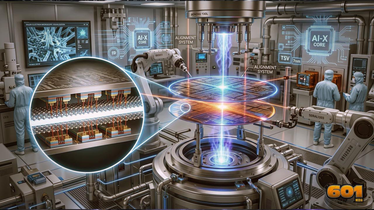
IBM addresses this problem with an entirely different manufacturing strategy. Rather than fabricating both transistors on the same wafer, engineers build them separately on two independent wafers. Each wafer undergoes its own manufacturing process before the finished structures are carefully joined together. This allows each transistor to be optimized without risking damage during subsequent processing.
The joining process, known as wafer bonding, depends on exceptionally smooth and clean silicon surfaces. When two atomically flat wafers are brought into close contact, tiny intermolecular attractions known as Van der Waals forces cause them to adhere. After controlled heating, stronger chemical bonds form, transforming the two individual wafers into a single integrated device.
Although the basic concept sounds simple, executing it is remarkably complex. Even microscopic particles invisible to the naked eye can prevent proper bonding, ruining weeks or even months of manufacturing work. As a result, semiconductor fabrication facilities maintain some of the cleanest environments ever created, ensuring dust contamination is virtually eliminated.
Alignment is equally demanding. Engineers must position billions of microscopic features on separate wafers with extraordinary precision before bonding occurs. Once the wafers touch, there is effectively no opportunity for correction. A slight misalignment can render the entire assembly unusable.
Interestingly, wafer bonding itself is not entirely new. Similar technologies are already found in several advanced electronic products. Modern smartphone camera sensors combine separate imaging and processing layers. High-bandwidth memory used alongside today’s AI processors stacks multiple memory layers to dramatically increase data transfer speeds. Flash storage devices also rely on vertical stacking techniques to maximize storage density.
IBM extends this established concept one step further by integrating the stacking process directly into the transistor architecture itself. This represents a significant shift in semiconductor engineering because it enables greater transistor density without relying exclusively on continued transistor shrinkage.
The company refers to this architecture as NanoStack. While it has been associated with a 0.7-nanometer technology demonstration, modern process-node numbers no longer describe the physical dimensions of individual transistors. Instead, these labels represent overall manufacturing generations and improvements in performance, efficiency, and density.
According to IBM’s projections, NanoStack technology could eventually deliver substantial improvements. The company estimates performance gains of up to 50 percent while reducing power consumption by approximately 70 percent. It also anticipates significantly denser SRAM memory, which is especially valuable for artificial intelligence workloads.
These potential benefits are particularly important because modern AI processors consume enormous amounts of energy moving data between memory and computing units. By placing memory and logic physically closer together through advanced stacking techniques, chips could reduce communication delays and lower overall power requirements.
Despite its promise, NanoStack remains a research demonstration rather than a commercial product. Developing an innovative architecture is only the first step. The true challenge lies in producing billions of these complex devices consistently, economically, and at industrial scale. Semiconductor history has repeatedly shown that successful mass manufacturing—not laboratory breakthroughs alone—determines whether a technology transforms the industry.
If wafer bonding can be perfected for large-scale transistor stacking, it may mark the beginning of a new chapter in chip development. Rather than asking how much smaller individual transistors can become, future engineers may focus on how efficiently they can arrange multiple silicon layers into a single, highly integrated computing system.
The next revolution in semiconductors may not come from shrinking the transistor itself. Instead, it may emerge from the invisible connection between two perfectly aligned silicon wafers, opening new possibilities for faster, more efficient computing in the years ahead.

I am a huge enthusiast for Computers, AI, SEO-SEM, VFX, and Digital Audio-Graphics-Video. I’m a digital entrepreneur since 1992. Articles include AI assisted research. Always Keep Learning! Notice: All content is published for educational and entertainment purposes only. NOT LIFE, HEALTH, SURVIVAL, FINANCIAL, BUSINESS, LEGAL OR ANY OTHER ADVICE. Learn more about Mark Mayo