

China’s EUV Breakthrough: The Long Road to Semiconductor Independence
China’s effort to develop its first domestically built Extreme Ultraviolet (EUV) lithography machine represents one of the most ambitious engineering projects in modern semiconductor history. Often compared to a national-scale technology initiative, the program aims to overcome years of export restrictions by recreating one of the world’s most sophisticated manufacturing systems from the ground up.
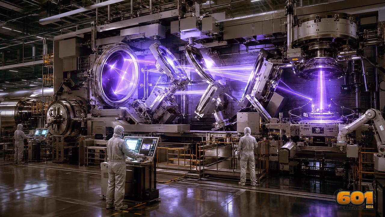
Unlike conventional manufacturing equipment, an EUV lithography machine enables the production of the smallest and most advanced semiconductor chips. It achieves this by using extremely short-wavelength light—13.5 nanometers—to print microscopic circuit patterns onto silicon wafers. Producing that light, however, is one of the greatest engineering challenges ever solved.
The industry leader, ASML, generates EUV light by firing high-powered lasers at 50,000 microscopic tin droplets every second. Each laser strike transforms the tin into plasma reaching temperatures of hundreds of thousands of degrees, producing the required EUV wavelength. The process demands extraordinary timing and precision, making it one of the most complex systems in modern manufacturing.
China appears to be pursuing two different strategies. Alongside a conventional laser-produced plasma approach similar to ASML’s design, researchers are also developing an alternative known as Laser-Induced Discharge Plasma (LDP). Instead of targeting rapidly moving tin droplets, LDP uses rotating tin-coated electrodes and powerful electrical discharges to generate plasma.
This alternative could simplify several mechanical challenges while reducing reliance on extremely high-precision laser targeting. However, previous attempts at LDP struggled to generate enough stable EUV power for commercial chip production. While recent reports suggest China has successfully demonstrated domestic EUV light sources using both approaches, their performance remains below the levels required for high-volume manufacturing.
Generating EUV light is only the beginning. Delivering that light to a silicon wafer presents another enormous obstacle. Ordinary lenses cannot be used because virtually every material absorbs EUV radiation. Instead, the entire optical system relies on an intricate series of multilayer mirrors capable of reflecting tiny amounts of EUV light with extraordinary precision.
These mirrors are among the most advanced optical components ever manufactured. Their surfaces must be polished to tolerances measured in picometers—smaller than the width of an atom—and coated with dozens of alternating layers of molybdenum and silicon. Even minor imperfections reduce efficiency, while each reflection loses a portion of the already limited light available.
For decades, Germany’s Zeiss has dominated this field through decades of accumulated expertise in polishing, coating, measuring, and aligning these specialized mirrors. Public reports indicate Chinese research institutes have now produced domestic EUV mirrors and integrated them into prototype optical systems. Although these mirrors have yet to match the optical quality, durability, and efficiency achieved by Zeiss, their successful integration marks a significant milestone in China’s development program.
One notable difference between China’s prototype and commercial ASML systems is its physical size. Reports suggest China’s machine occupies an entire factory floor, far exceeding the footprint of existing production scanners. This larger scale may reflect a deliberate engineering compromise. By using larger optical components, longer beam paths, and larger collectors, engineers may compensate for lower mirror efficiency and reduced light output without requiring the same level of precision achieved by current commercial systems.
Beyond engineering challenges, the project also depends on critical materials. Helium plays an essential role throughout semiconductor manufacturing by cooling equipment, protecting sensitive components, and detecting microscopic leaks. Despite its importance, China imports the vast majority of its helium supply, creating another strategic dependency. Since helium cannot be easily stored for extended periods and global supplies remain concentrated in only a few countries, securing reliable access has become an important consideration for any domestic semiconductor ecosystem.
Recognizing that advanced technology depends not only on hardware but also on human expertise, China has significantly expanded investment in semiconductor research while encouraging experienced engineers working abroad to return home. Research activity surrounding EUV lithography has increased substantially since 2020, with numerous institutions simultaneously tackling different portions of the technological challenge.
Current reports suggest China’s prototype EUV machine produces approximately 100 watts of EUV power, compared to roughly 300 watts generated by today’s commercial ASML systems and more than 700 watts achieved by newer prototypes. Although this gap remains significant, complete parity may not be China’s immediate objective.
Today, China’s most advanced semiconductor manufacturing still relies heavily on older Deep Ultraviolet (DUV) lithography using multiple exposure techniques. This approach increases manufacturing complexity, reduces yields, and raises production costs. Even a domestic EUV system that falls short of international leaders could provide substantial improvements by reducing dependence on repeated DUV processing.
The journey from a functioning laboratory prototype to a reliable production tool remains lengthy. Commercial EUV systems require years of refinement before achieving the reliability needed for around-the-clock operation in semiconductor fabrication plants. Nevertheless, China’s reported progress demonstrates that rebuilding an advanced lithography ecosystem involves far more than replicating individual components. It requires developing expertise across optics, plasma physics, materials science, precision engineering, and manufacturing integration.
Ultimately, the significance of China’s EUV program lies not only in technological competition but also in its pursuit of long-term semiconductor self-sufficiency. Success will depend less on matching every benchmark set by existing industry leaders and more on building a dependable domestic capability capable of supporting the nation’s growing semiconductor industry.

I am a huge enthusiast for Computers, AI, SEO-SEM, VFX, and Digital Audio-Graphics-Video. I’m a digital entrepreneur since 1992. Articles include AI assisted research. Always Keep Learning! Notice: All content is published for educational and entertainment purposes only. NOT LIFE, HEALTH, SURVIVAL, FINANCIAL, BUSINESS, LEGAL OR ANY OTHER ADVICE. Learn more about Mark Mayo